PCBA Development
Control board design, SMT assembly, firmware integration and functional test.
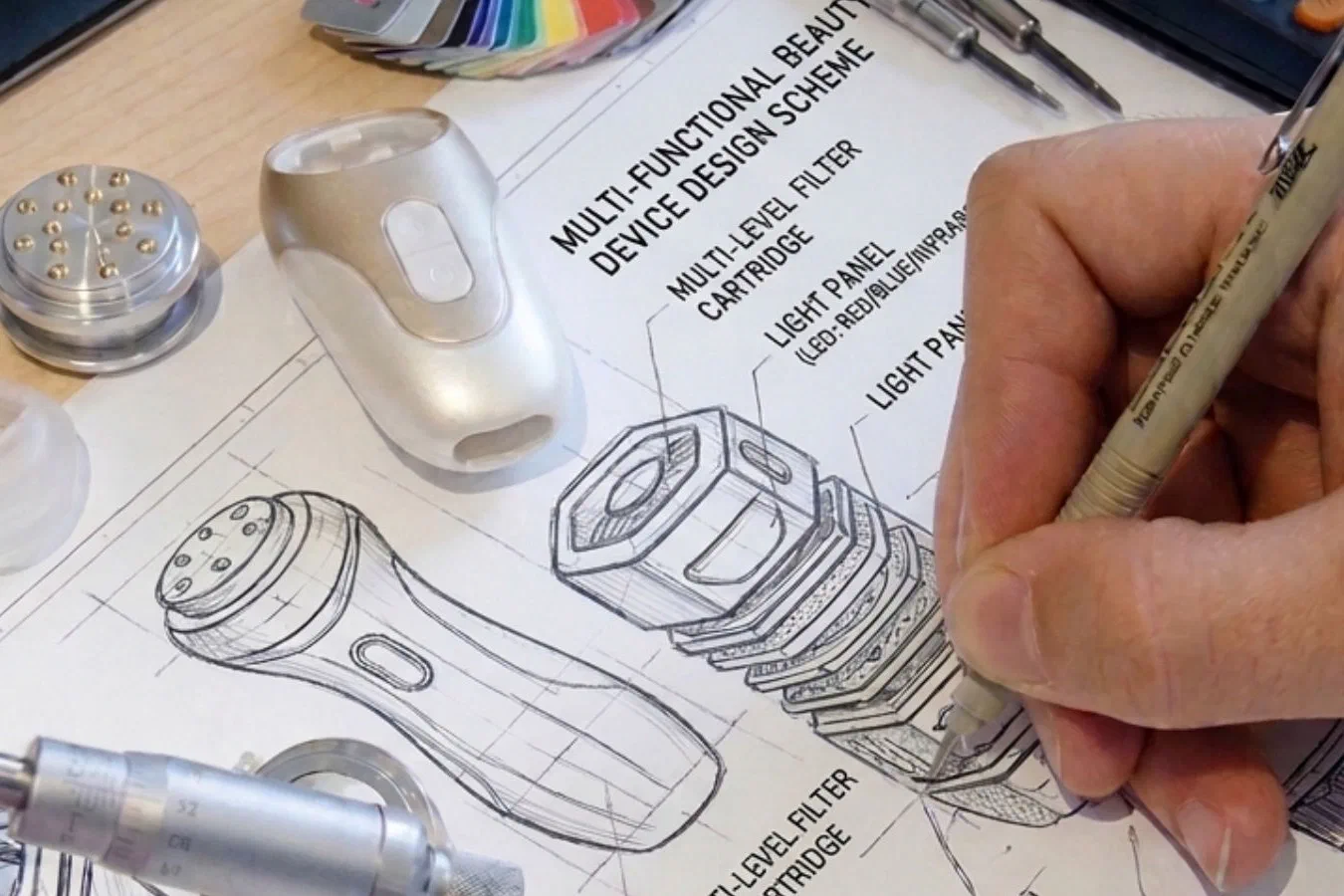
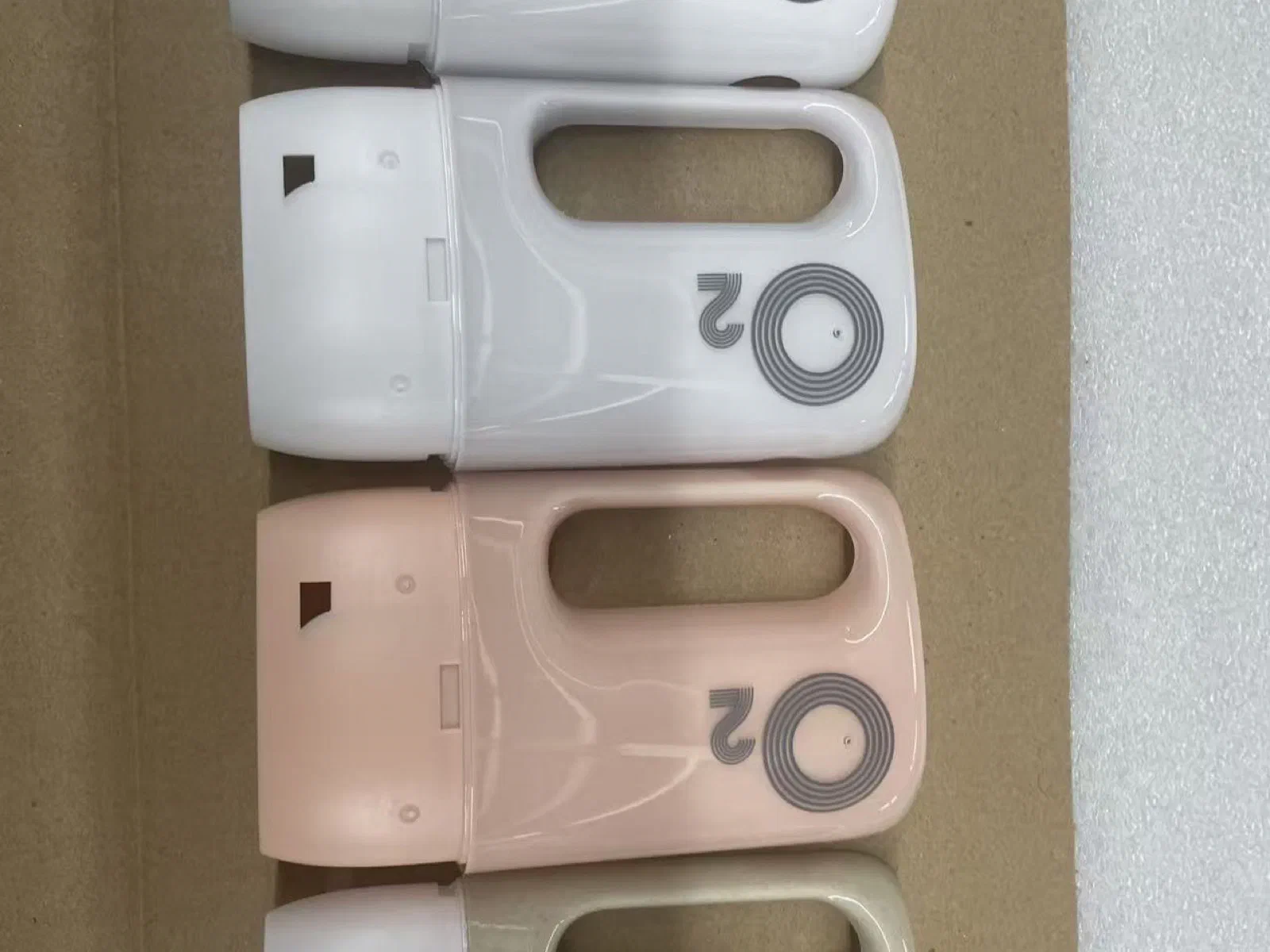
Control boards are designed and assembled in the same building as the housing. For new designs we define the electronics architecture alongside the mechanism, so battery, charging, sensing and output control are designed as one system rather than bolted on afterwards.
Where boards fail
Most field failures on a beauty device are not exotic: a battery protection threshold set too close to the charger’s tolerance, a connector that fatigues after a few hundred flex cycles, a firmware state machine that never leaves the highest intensity. These are design decisions, and they are cheapest to fix before the first panel is ordered.
From design to line
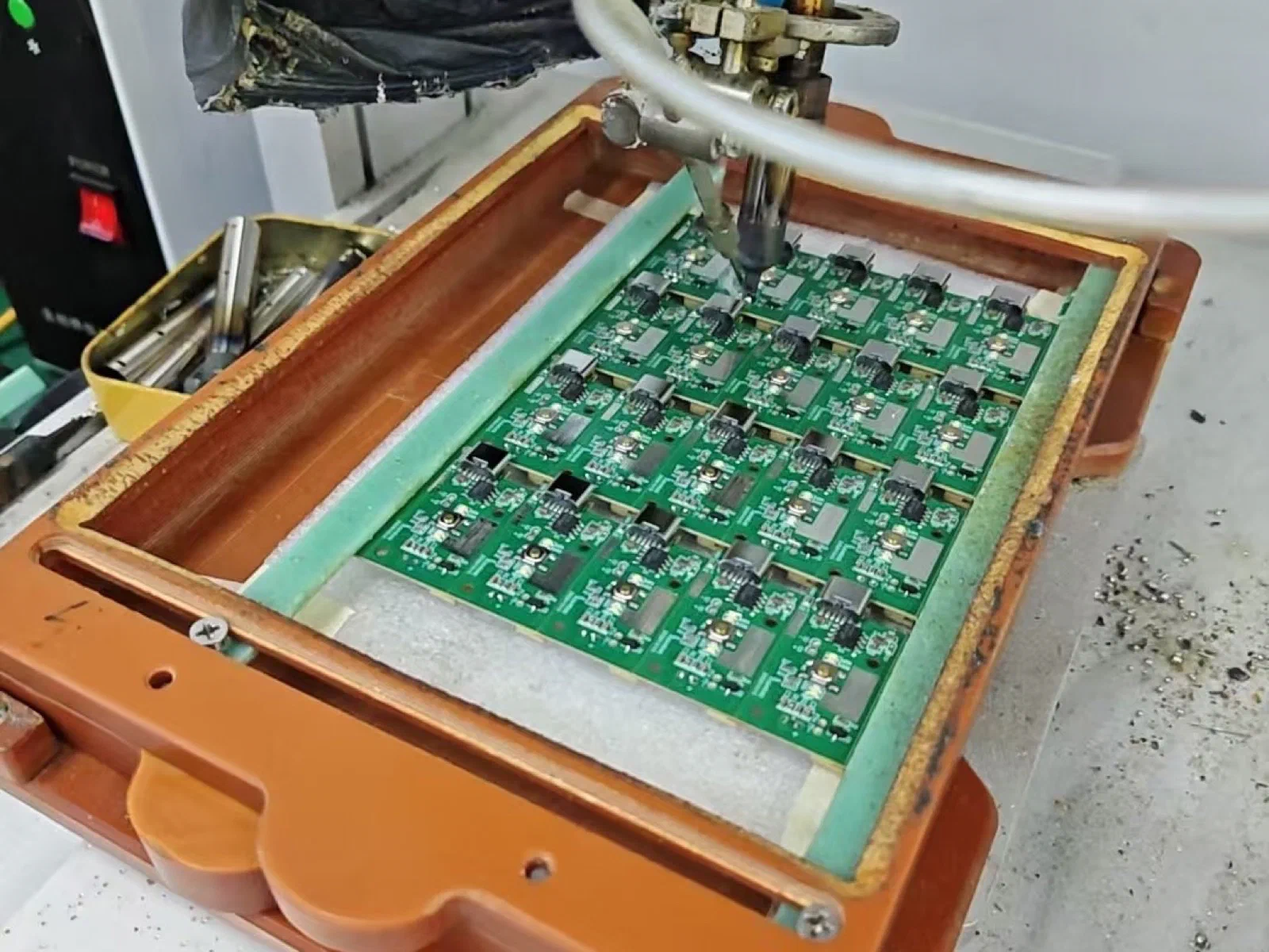
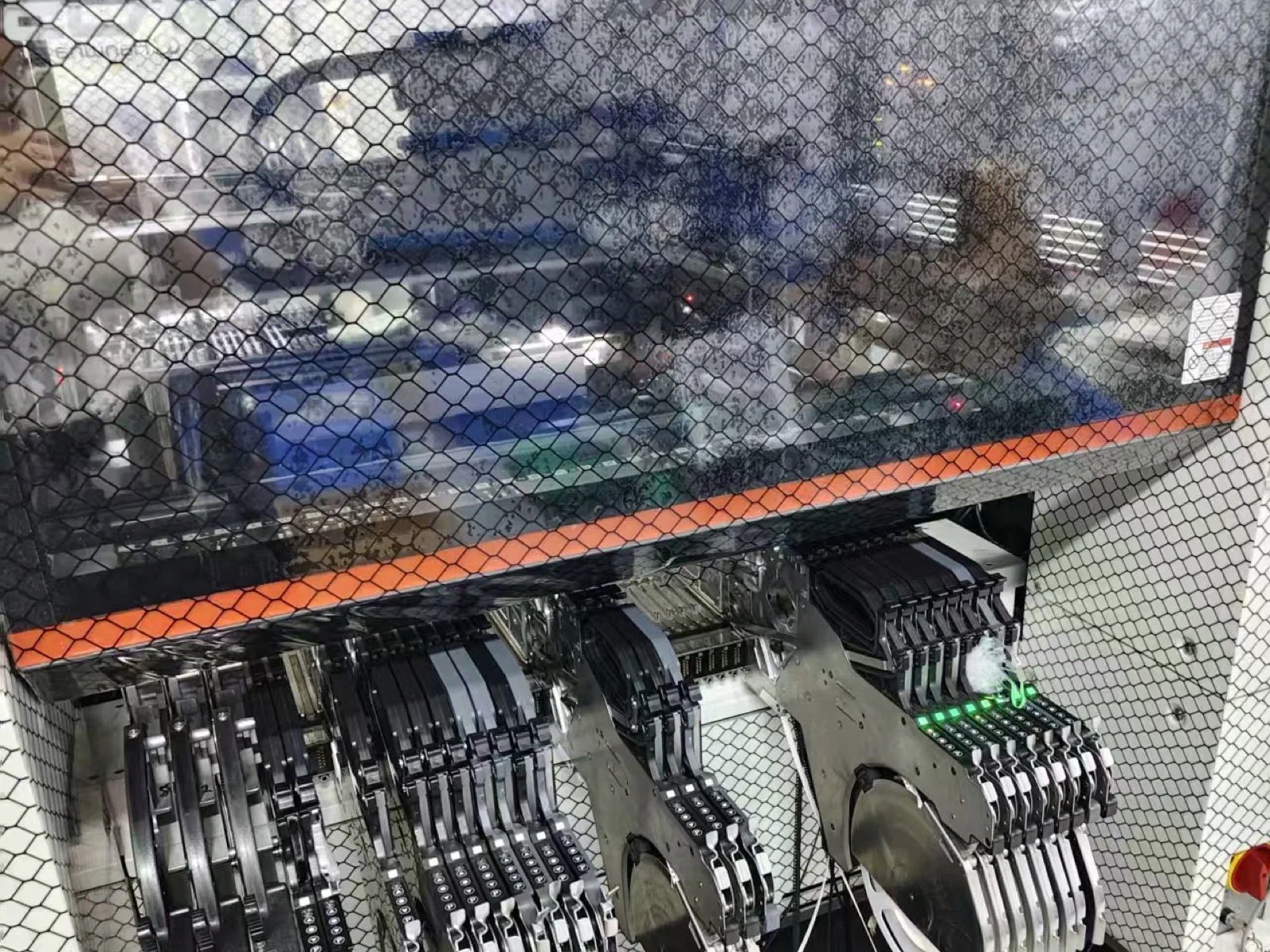
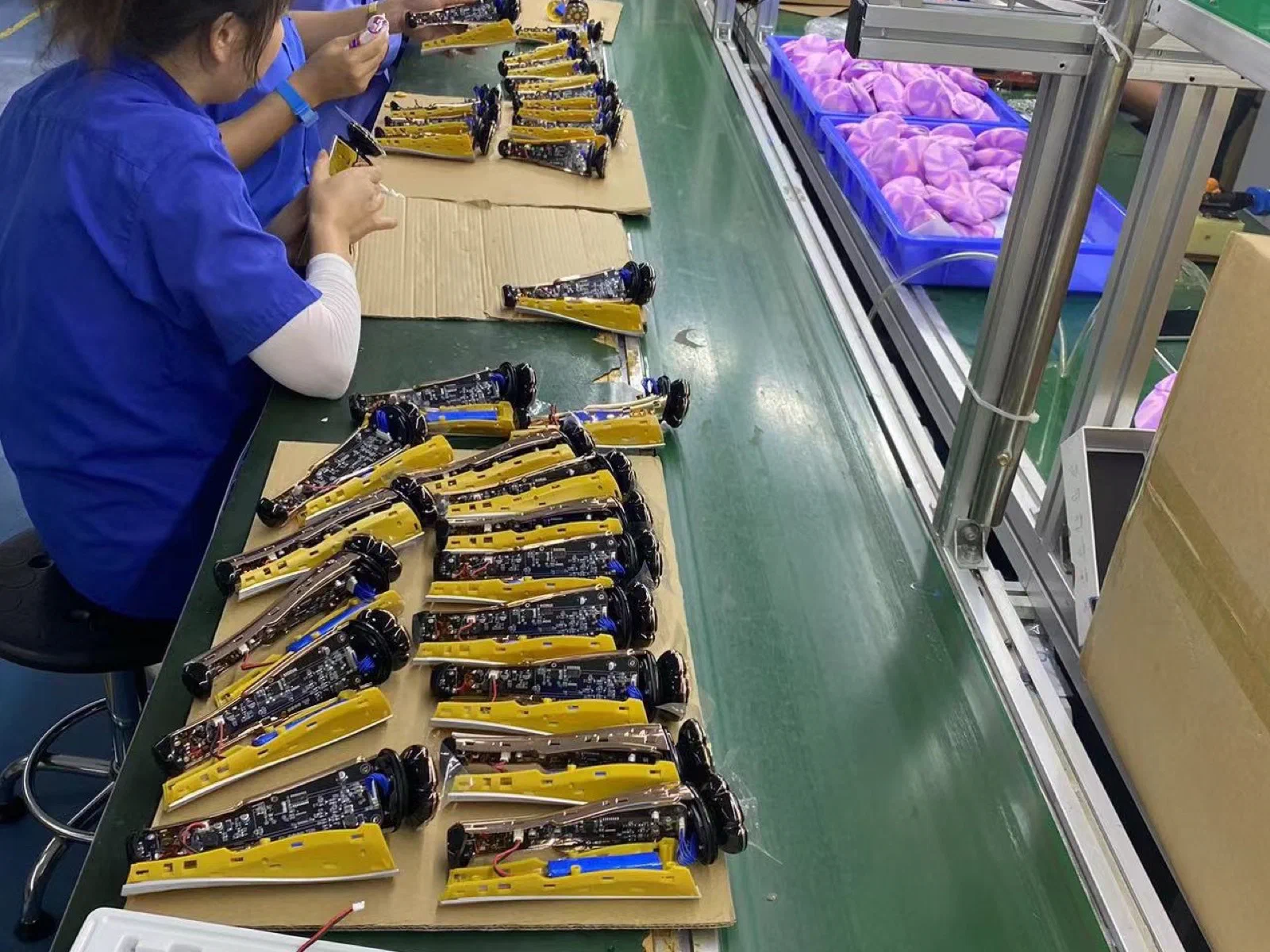
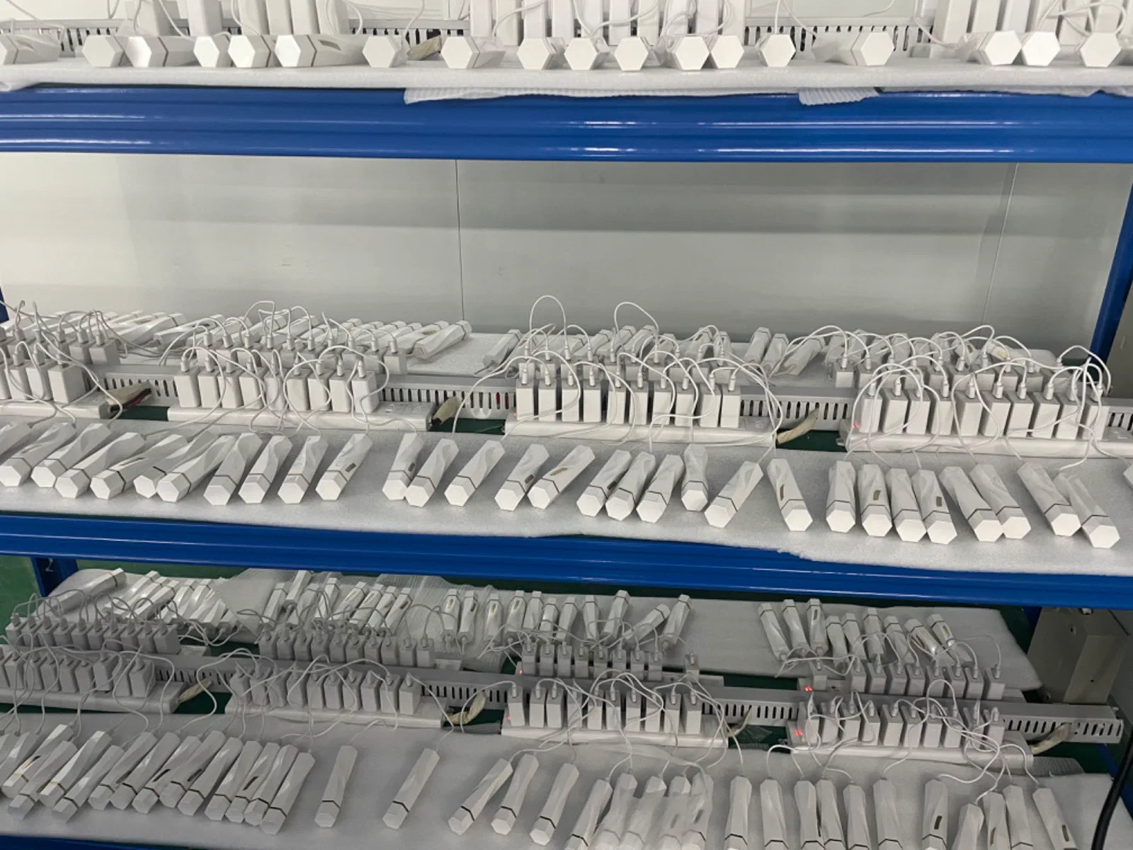
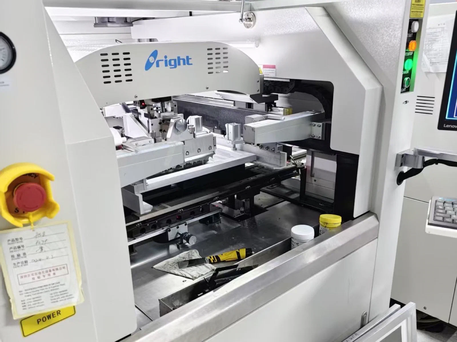
Boards are placed, reflowed and selectively soldered in-house, then functionally tested before they reach assembly. A failed board is repaired and retested rather than quietly packed; the test record stays with the batch, so a return can be traced to the board rather than to the whole shipment.
Certification is designed in
For the LKL2315 platform we hold CE-EMC (EN 55014), FCC SDoC and RoHS reports, and the certificate numbers are published rather than summarised. An EMC pre-scan runs before the formal test, because the useful moment to discover a margin problem is while the layout can still change.
At a glance
- In-house equipment
- 3 SMT machines, solder paste printing, reflow and selective soldering
- Scope
- Schematic, layout, firmware, programming and functional test
- Design reviews
- Power budget, thermal margin, battery protection and EMC review before the first board is ordered
- Functional test
- Every board is tested before it reaches the assembly line; failed boards are repaired and retested
- Evidence
- CE-EMC, FCC SDoC and RoHS reports for LKL2315, with report numbers published on the certification page
What you get